ExplainMultiplexingEnglish
| project overview | |

| |
| Year | 2017 |
| Number of pixels | 40 |
| Grayscales / Colors | on/off |
| Illuminant | 3 mm LEDs |
| Power input | |
| Contact person | Arne Rossius |
| Project website | |
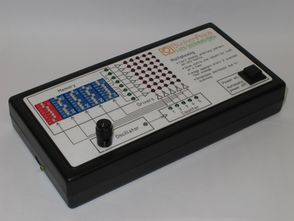
Explain: Multiplexing is a small box to demonstrate the concept of multiplexing. It contains an oscillator with user-adjustable speed, a column counter, a DIP-switch "memory" for the pattern to be displayed and the actual matrix of multiplexed LEDs itself. The front is covered with a printed block diagram of the connections between the components and some explanations.
The main circuit only two standard ICs and no programmable parts, so even the circuit is easy to understand. An additional IC is used to charge the internal lithium-polymer battery. To ensure maximum battery lifetime, an auto-power-off circuit is used to shut off the circuitry after approx. 5 minutes. This means the Explain can survive an entire CCC congress without needing to be recharged.
Electronics
Oscillator
The oscillator generates the timing pulses for the multiplexing. With every timing pulse, the multiplexing steps to the next column in sequence. The speed can be adjusted with a potentiometer.
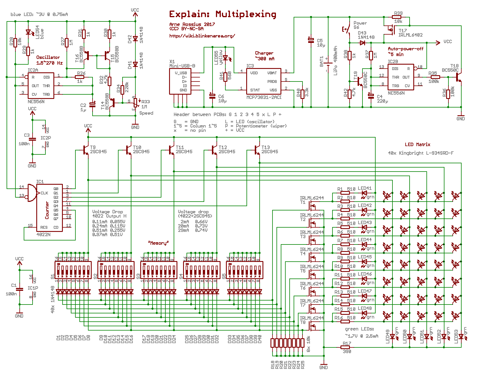
One half of a NE556 dual timer IC (two NE555 circuits on one chip) is used as the basis. To make the speed adjustment "feel" linear to the user, the actual change needs to be reverse logarithmic. As reverse-logarithmic taper potentiometers are hard to find, a standard linear potentiometer was modified by adding a resistor between two terminals. This modification only works if the potentiometer is used as a voltage divider, but all typical NE555 oscillator configurations need a rheostat instead. To solve this issue, the potentiometer is used instead to generate a variable voltage, which is buffered by an emitter follower (T14), converted to a current by a resistor (R32) and then mirrored (T15, T16, R30, R31) to be used as a charge current for the capacitor C2. Two diodes (D41, D42) limit the adjustment range of the potentiometer, as both the emitter follower and the current mirror need one diode drop of voltage to operate. To avoid the oscillator stopping entirely if there is a slight mismatch between the voltage drop across the actual diodes and the transistor B-E diodes, a large resistor (R27) provides a minimum charge current.
When the capacitor is charged to 2/3 of the supply voltage, the NE556 connects its discharge pin (DIS) to ground and quickly discharges the capacitor. At the same time, the output pin (OUT) also goes low. Once the capacitor voltage has dropped below 1/3 of the supply voltage, the discharge pin returns to open circuit and the output becomes high again. As the discharge resistor (R26) is small compared to the charge current provided by the current mirror, the capacitor discharge time hardly varies with the speed setting.
A blue LED (LED54) on the oscillator's output lights up during each pulse. As the pulses are very short, the LED needs to be quite bright to make the pulses sufficiently visible even at the slowest speed setting. As super-bright LEDs often have a narrow beam angle, it was lightly sanded to diffuse the light better.
Counter and Column Buffers
The negative output pulses of the oscillator are used to clock a 4022 counter IC. It is similar to the more well-known 4017, but only provides 8 outputs. As this circuit only needs 5 outputs, either IC can be used. As the clock pulses are negative going, the output of the oscillator is connected to the inverted clock input (sometimes described as the "#Enable" input) rather than the non-inverted clock input. The first unused output of the counter is connected to its reset input to restart the sequence.
The output current of CMOS ICs is very low, so the five outputs of the counter are connected to emitter followers acting as buffers. The 2SC945 transistors were chosen over the more common BC54x or BC337 types for their more convenient pinout (collector in the middle). The buffers drive the inputs to the DIP switch "memory", the columns of the LED matrix (active high), and one additional LED each to show which column is active (LEDs 49~53). A single current limiting resistor for all 5 LEDs is sufficient as only one of them is lit at any time.
Memory and Row Buffers
The memory is simply an array of DIP switches to allow the user to quickly adjust the displayed pattern. The positioning of the switches on the board matches the arrangement of the LEDs, so it is easy to see the correspondence between the DIP switch setting and the displayed pattern. Each switch has a diode in series to allow the outputs to be connected together without feeding one switch's signal back to another column output through another switch. Eight pull-down resistors pull the memory outputs low if the switch for the active column is off.
The outputs from the memory are fed to eight MOSFET drivers. Bipolar transistors could be used instead, but base resistors would need to be added. The buffering of the signals isn't strictly necessary as the memory inputs are already fed from the buffered column signals, and both the switches and the diodes can easily handle the currents to drive the LED array. However, since the columns are driven with active-high signals, the rows must be driven with active-low signals to make the LEDs light up. The MOSFETs invert the (active-high) input signals from the memory and provide the active-low outputs for the LEDs.
Only one column lights up at a time, but several rows in that column may be on simultaneously. This means the current limiting resistors for the LED array must be placed in series with the row signals, to avoid a single resistor being shared by more than one active LED at the same time, which would result in changing brightness depending on the number of LEDs switched on at the same time.
In addition to the LED array, an additional column of 8 additional LEDs (LEDs 41~48) is used to show which rows are being driven at any given time.
Auto-Power-Off
The auto-power-off circuit uses the second half of the NE556 IC. After conncting the battery, the circuit will remain unpowered as the main switch MOSFET (T17) isn't conducting. When the power-on button (S6) is pushed, the circuit is powered up through D43. At the same time, R38 turns on T19, which discharges the timing capcitor C4. With both of its inputs low, the NE556 sets its output high, which turns on T18, which pulls down the gate of the MOSFET, which turns on and supplies the circuit with power.
When the power button is released, C4 starts charging slowly through R37. When the voltage on it reaches 2/3 of the supply voltage, the NE556 changes its output to low, turning off T18, which stops pulling the MOSFET's gate low. Instead, the gate is pulled high by R39 and the circuit turns off.
The charge time until power off can be approximated by calculating the time constant &tau&bnbsp;=&bnbsp;R&bnbsp;*&bnbsp;C. Tau corresponds to a ~63.2% charge, which is fairly close to the 2/3 (~66.7%) charge required. The values of 1 MΩ and 220 μF give Tau = 220 s or ~3.7 Minutes. As the real capacitor has a large tolerance and the circuit will have some leakage currents, the actual turn-off time measured was closer to 5 minutes.
Battery Charging
IC3 is a specialised battery charger IC for lithium-polymer batteries. The charge current is programmed with R40. LED55 lights up while the battery is charged and turns off when the battery is fully charged or if there is no input voltage on the USB connector.
Photos
More photos here: http://arne.blinkenarea.org/explain_multiplexing/
